Home⁄ Facilities⁄ Instruments⁄ User Instruments⁄ Mechanical Properties Testing and Analysis⁄ Micro Hardness Tester
Micro Hardness Tester
 Bard Hall B56
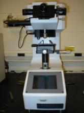
Indentation measuring modes include Vickers, Knoop and Brinell. Ideal for testing on a wide range of materials, including plating. Rigid construction minimizes compliance errors and an internal memory retains 999 tests. A highly stable load mechanism ensures accurate positioning. Once the load is selected automatic testing begins, including loading, holding and releasing, for highly magnified measurements. Upon completion the turret revolves automatically; switching position from the indenter to an optical microscope. Repositioning accuracy is <0.5 micron. The standard incorporated microscope includes X10 and X40 total magnifications. Loads range from 9 to 20000 millinewtons.
Operating Instruction Manual Application
For rates information, please see the rates page.
Primary Contact

Mark Pfeifer
(607) 255-4161
map322@cornell.edu
Bard Hall, Room B-57
Mark Pfeifer
(607) 255-4161
map322@cornell.edu
Bard Hall, Room B-57