Electron microscopy shows ‘mouse bite’ defects in semiconductors
March 3, 2026
News
Note: This news item features content from another page. View the featured content for this news item.
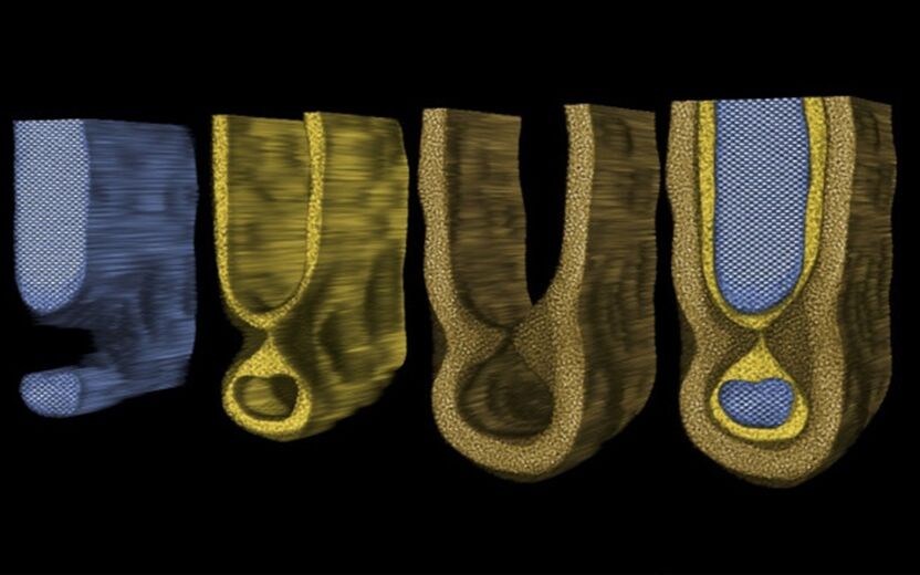
Cornell researchers utilized advanced electron microscopy to identify "mouse bite" defects—microscopic edge irregularities that cause increased resistance and heat in semiconductors. This discovery allows manufacturers to refine etching techniques to improve the precision and efficiency of next-generation microchips.