Electron and Optical Microscopy and Imaging
Scanning Electron Microscopy (SEM)
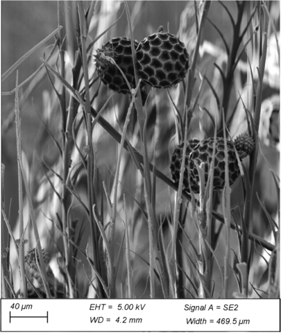
pollen stuck in bee leg hairs (scopae). Credit: Nathalia Florez Gomez
SEM offers high-resolution imaging of many sample types. All of our SEMs can identify and quantify elements with energy-dispersive X-ray spectroscopy (EDX, also referred to as EDS) detectors. Depending on the instrument, other capabilities may include elemental mapping, ultra-low voltage operation for enhanced surface contrast, electron backscatter diffraction (EBSD) for crystallographic orientation analysis, low-vacuum imaging, beam deceleration modes, and transmitted electron imaging for thin specimens. Highlighted text in the drop-down details below indicates a feature unique to that specific SEM. Click here to see some imaging capabilities of our SEMs.
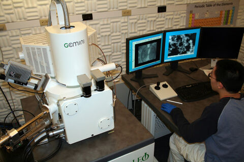
Zeiss Gemini 500 SEM
Primary staff: Mick Thomas; secondary: Alicia Tripp
Location: Clark Hall F3

- Load-lock for fast sample pump-down time
- Optimized for low and ultra-low voltage imaging (3keV down to 200eV)
- In-lens and Everhart-Thornley secondary electron (SE) detectors
- In-column, scintillator-based and semiconductor-based backscatter (BSE) detectors
- Low-vacuum imaging of insulating samples
- Scanning transmission (STEM) imaging of very thin specimens
- Energy-dispersive X-ray detector (EDX) for elemental analysis and X-ray mapping
Zeiss Sigma 500 SEM
Primary staff: Mark Pfeifer, Kevin Silverstein; secondary: Phil Carubia
Location: Bard Hall SB56
- Load-lock for fast sample pump-down time
- Optimized for low and ultra-low voltage imaging
- In-lens and Everhart-Thornley secondary electron (SE) detectors
- Scintillator-based backscatter detector
- Energy-dispersive X-ray (EDX) detector for elemental analysis and X-ray mapping
- Electron Back-Scattered diffraction (EBSD) detector to analyze crystallographic structure of materials
Tescan Mira SEM
Primary staff: Kevin Silverstein, Mark Pfeifer; secondary: Phil Carubia
Location: Bard Hall B-47B
- Optimized for low voltage imaging and ultra-low voltage imaging using beam deceleration
- In-lens and Everhart-Thornley secondary electron (SE) detectors
- Scintillator-based backscatter detector
- Energy-dispersive X-ray detector (EDX) for elemental analysis and X-ray mapping
Zeiss LEO 1550 (Keck) SEM
Primary staff: Mick Thomas; secondary: Alicia Tripp
Location: Clark Hall F3
- Imaging at very high resolution (1 nm at 20 keV and 2.5 nm at 5 keV)
- Optimized for low voltage imaging (0.5 to 3 kV)
- In-lens secondary electron (SE) detector
- Energy-dispersive X-ray detector (EDX) for elemental analysis and X-ray mapping
Transmission Electron Microscopy (TEM)
Advanced TEM, Scanning Transmission Electron Microscopy (STEM), Cryo-STEM, and Cryo-TEM capabilities provide atomic-resolution imaging, spectroscopy, and tomography across both material and biological sciences. Capabilities include 5th order aberration correction; aberration corrected field-free Lorentz imaging of magnetic domains; spectral imaging including both electron energy loss spectroscopy (EELS) and energy dispersive X-ray spectroscopy (EDX); and cryogenic operation for structural preservation. Most microscopes support multiple imaging modes including: brightfield and darkfield TEM and STEM; center of mass (COM) or differential phase contrast (DPC) imaging; pixelated detectors for acquiring 4DSTEM and ptychographic data; energy filtered TEM (EFTEM); selected area diffraction; tomography; and Lorentz imaging. We have automation tools for high-throughput acquisition and on-the-fly processing of single-particle cryo-EM data and can assist with other reconstructions. If you have any interest in or questions about TEM/STEM, please contact any of our managers; we are happy to help.
Transmission Electron Microscopes (TEM)
Thermo Fisher Talos Arctica
Primary staff: Mariena Silvestry Ramos; secondary: Phil Carubia, Mick Thomas
Location: Physical Sciences Building B05
The 200kV Arctica TEM is optimized for high-throughput, high-resolution imaging for single particle cryo-EM. A full description for this instrument can be found at Thermo Fisher Talos Arctica.
Thermo Fisher Talos F200C
Primary staff: Mariena Silvestry Ramos; secondary: Phil Carubia, Mick Thomas
Location: Physical Sciences Building B71
The Thermo Fisher Talos F200C transmission electron microscope (TEM) provides 2-D and 3-D characterization of biological samples in cell and structural biology as well as other soft materials. It is an easy-to-use general-purpose TEM. A full description for this instrument can be found at Thermo Fisher Talos F200C.
Scanning Transmission Electron Microscopes (STEM)
Thermo Fisher Spectra 300 (Andromeda)
Primary staff: Phil Carubia; secondary: John Grazul, Mick Thomas
Location: Duffield Hall 150
The Spectra 300 (Andromeda) is a Scanning Transmission Electron Microscope (STEM) for ultra-high-resolution imaging and composition analysis. A full description for this instrument can be found at Thermo Fisher Spectra 300 (Andromeda).
Thermo Fisher Spectra 300 (Kraken)
Primary staff: John Grazul; secondary: Phil Carubia, Mick Thomas
Location: Duffield Hall 150
The Spectra 300 (Kraken) is a Scanning Transmission Electron Microscope (STEM) for ultra-high-resolution imaging and composition analysis. A full description for this instrument can be found at Thermo Fisher Spectra 300 (Kraken).
Thermo Fisher Titan Themis (Cryo-STEM)
Primary staff: Phil Carubia; secondary staff: Mariena Silvestry Ramos, Mick Thomas
Location: Physical Sciences Building B91
The Cryo-S/TEM bridges the fields of materials and biological sciences, providing a unique platform to conduct interdisciplinary research (biology, engineering, chemistry, and physics) at atomic resolution. Samples ranging from rechargeable batteries and crystals to isolated proteins and cells can be imaged seamlessly. A full description for this instrument can be found at Thermo Fisher Titan Themis (Cryo-STEM).
Thermo Fisher Titan 300 (Perseus)
Primary staff: John Grazul; secondary: Phil Carubia, Mick Thomas
Location: Duffield Hall 150
The Perseus STEM is a general-purpose, high-resolution microscope for imaging and analysis of a broad range of materials and biological samples. A full description for this instrument can be found at Thermo Fisher Titan 300 (Perseus).
Sample Preparation Tools
Focused ion beam (FIB) instruments are used for TEM sample preparation utilizing precise milling, cross-sectioning, and site-specific preparation. FIBs support automated TEM workflows and cryogenic lift-out for sensitive materials, including full cryo-TEM cross-section preparation. Additionally, the CCMR has a range of electron microscopy (EM) sample prep tools such as sputter coaters, diamond saws, polishers, microtomes, a critical point dryer, and an ion mill.
Thermo Scientific Helios G4-UX FIB
Primary staff: Mick Thomas; secondary: Phil Carubia
Location: Duffield Hall 150
- High resolution secondary and backscattered imaging even at low voltages
- High resolution ion beam imaging, down to 2keV
- Low-voltage milling capability produces high quality TEM lamella
- Energy-dispersive X-ray (EDX) detector for elemental analysis and X-ray mapping
- Deposition sources (platinum and carbon)
- High-stability EasyLift EX Nano Manipulator for TEM sample prep, sample modification, and localized grounding for work on insulating materials
- Auto TEM software to reduce the time needed to make TEM lamella
To acknowledge: This work made use of a Helios FIB supported by NSF (DMR-1539918) and the Cornell Center for Materials Research Shared Facilities.
Tescan Amber X Plasma FIB (PFIB) (coming Summer 2025)
To be installed Summer 2025.
Primary staff: Phil Carubia; secondary: Mick Thomas
Location: Physical Sciences Building B95
- High throughput, large area FIB processing up to 1 mm
- Ga-free microsample preparation
- Ultra-high resolution, field-free FEG-SEM imaging and analysis
- In-lens SE and BSE detection
- Resolution optimization for high-throughput, multi-modal FIB-SEM tomography
- Superior field of view for easy navigation
- Essence™ easy-to-use, modular graphical user interface
- Cryo capabilities
Thermo Scientific Strata 400S
Primary staff: Mick Thomas; secondary: Phil Carubia
Location: Physical Sciences Building B95
- High resolution secondary and backscattered electron imaging
- High resolution ion beam imaging down to 5keV
- Low-voltage (2keV) ion milling capability to produce high quality TEM lamella
- Oxford energy-dispersive X-ray (EDX) detector for elemental analysis and X-ray mapping
- Deposition sources (platinum and carbon)
- Omniprobe manipulator for TEM sample prep, sample modification, and localized grounding for work on insulating materials
- Cryo capabilities for imaging, milling, and TEM lamella
Thermo Scientific Vitrobot Mark IV System
Primary staff: Mariena Silvestry Ramos
Location: Clark Hall D21E
Training is done by Katie Spoth or Mariena Silvestry. Upon successful completion of the training, users can access the Vitrobot at all times with their ID.
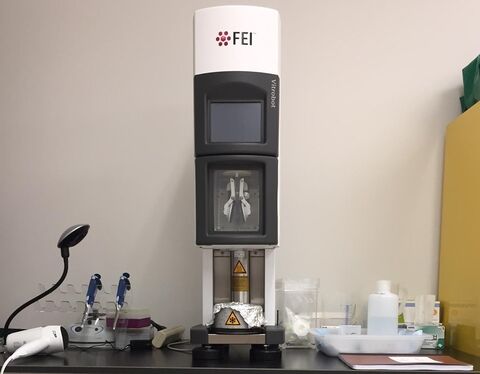
A set of Vitrobot tweezers is provided, but users are always welcome to bring their own. Two glow discharge/plasma cleaner units are available for use, along with a storage dewar for temporary sample storage. Users must bring their own grids and grid boxes prior to using the instrument, especially for their first training session. Contact Mariena or Katie for information on what supplies are needed for sample vitrification.
- Highly automated system with enclosed process chamber
- Maintains constant physical and mechanical conditions such as temperature, relative humidity, blotting conditions, and freezing velocity during cryo-fixation process
- Precisely timed control of multiple sample applications, blotting actions, and vitrification
Additional EM Sample Preparation Tools
Primary staff: John Grazul; secondary: Mick Thomas
Location: Duffield Hall 231
- Allied HighTech High Speed Saw
- Allied HighTech Low Speed Saw
- Allied Multiprep Polishers
- Critical Point Dryer
- Fischione 1010 Ion Mill
- Leica Ultracut UCT Microtome
- Leica EM UC7/FC7 Cryo-Ultra-microtome
- Sputter Coaters (carbon and Au-Pd)
- Cryo microtome
- Vibratory microtome
- Freeze dryer
- Electrolytic polisher
- Dimpler
Confocal and Conventional Optical Microscopes
Confocal microscopy utilizes a pinhole before the photodetector to reject out-of-focus light which produces sharp images with high resolution, and 3D reconstructions of the imaged area can be produced through z-stacking. For conventional microscopy, we have several Olympus microscopes in each facility that have varying types of objectives, polarizers, and image capture systems.
Confocal Microscopes:
3i Marianas Spinning Disk Confocal Microscope
Primary staff: Alicia Tripp; secondary: Steve Kriske
Location: Clark Hall D21B
The 3i (Intelligent Imaging Innovations) Marianas Spinning Disk Confocal fluorescence microscope is perfect for gently imaging live samples as well as samples with large optical fields of view. With a fully motorized precision stage and fast acquisition, the inverted microscope is equipped for automating data collection from multiple locations, assembling 3D data sets, and collecting time-lapse videos. The SlideBook software works seamlessly for powerful and intuitive image analysis and allows many options for data export.
Setup Includes:
- Zeiss Axio Observer 7 Advanced Marianas™ Microscope
- Inverted Microscope with Transmitted Light LED Illuminator
- Motorized Nosepiece and X,Y Stage
- Objectives: 10x (air) ; 100x (oil)
- Yokogawa CSU-X1 A1H Spinning Disk Confocal Scanning Unit
- Up to 2,000 fps Scanning Speed
- Bandpass Filters: 617/73; 445/45; 525/30
- Evolve 512 Delta 20MHz Back Illuminated EMCCD Camera
- LaserStack with laser lines: 405 nm; 488 nm; 532 nm; 561 nm
Keyence VK-X260 Profilometer
Primary staff: Alicia Tripp; secondary: Steve Kriske
Location: Clark Hall D15
The Keyence is a confocal laser profilometer that utilizes in-focus reflections from a 408 nm laser source to obtain 3D images of material surfaces.
A full description for this instrument is located on the Surface Analysis Instrumentation page.
WITec Alpha300R Confocal Raman Microscope
Primary staff: Kevin Silverstein; secondary: Mark Pfeifer
Location: Bard Hall SB30
The Alpha300R can be used to investigate existing chemistry, track chemical bonds through a process, investigate crystallinity, image strain fields, and measure photoluminescence.
A full description for this instrument is located on the Vibrational Spectroscopy page.
Renishaw InVia Confocal Raman Microscope
Primary staff: Kevin Silverstein; secondary: Mark Pfeifer
Location: Bard Hall SB30
The Renishaw InVia can be used to investigate existing chemistry, track chemical bonds through a process, investigate crystallinity, image strain fields, and measure photoluminescence.
A full description for this instrument is located on the Vibrational Spectroscopy page.
Conventional Microscopes:
Olympus BX51 with Crossed Polarization
Primary staff: John Grazul
Location: Duffield Hall 231
Using reflected or transmitted light, this microscope produces excellent images which may be recorded using our Olympus digital camera. We have objectives for longer working distances and for samples under a coverslip or without a coverslip. The stage rotates, which is useful when using the crossed polarization mode for the observation of geological thin sections.
Olympus BH-2 with Darkfield
Primary staff: John Grazul
Location: Duffield Hall 231
Darkfield light microscopy highlights subtle surface features by only allowing illumination from low angles to reach the specimen. There is an alternative bright fluorescence attachment for this microscope and the digital camera can be used to record images. Magnifications of 50x to 400x are available and the microscope is primarily designed for reflected light.
Olympus BX53M
Primary staff: Alicia Tripp, Steve Kriske
Location: Clark D21B
A semi-motorized microscope with high-performance X Line™ objectives (5x, 10x, 20x, 50x, 100x) with bright LED lighting. Sharp and high-resolution images with good color accuracy are easily obtained with this microscope.