Home⁄ About⁄ News⁄ FEI and Cornell Collaborating on new EMPAD Detector
FEI and Cornell Collaborating on new EMPAD Detector
FEI and Cornell University Collaborate to Commercialize New EMPAD Detector
April 7, 2017 Cornell Chronicle article
Speed, sensitivity and dynamic range will enable multichannel atomic-scale imaging and analysis of material properties such as electric and magnetic fields. This development is being supported by the CCMR and the Kavli Institute at Cornell. For further information, see this poster [link to PDF of poster] and the FEI announcement below (link to https://www. fei.com/news/FEI-and-Cornell-University-Collaborate-to-Commercialize-New-EMPAD-Detector/).
Hillsboro, Ore. and Ithaca, NY/July 25, 2016 – FEI and Cornell University have entered an agreement to commercialize a new high dynamic range detector for FEI’s electron microscopes. It promises to enable new kinds of multichannel imaging and analysis that have not been possible previously. FEI expects to complete the commercialization of the design and offer the detector for new and retrofitted electron microscopes in 2017.
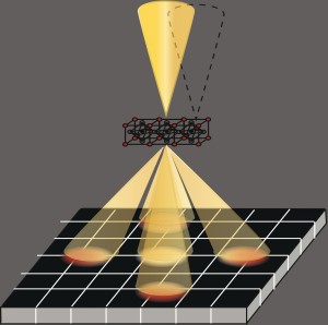
Uniquely, the electron microscope pixel array detector (EMPAD) simultaneously captures the spatially and angularly-resolved distribution of all transmitted electrons, allowing researchers to acquire and post-process a complete data array of scattering information to generate images and analytical results in scanning transmission electron microscope (STEM) applications. Atomic resolution image contrast enhancement methods, such as iDPC, electric and magnetic field visualizations, and strain measurement techniques, will benefit from the unmatched performance of the new detector.
“The EMPAD records an image frame in less than a millisecond, and can detect from 1 to 1,000,000 primary electrons per pixel, per image frame,” explained Professor David Muller, School of Applied and Engineering Physics, Cornell University. “This is 1000x the dynamic range, and 100x the speed of conventional electron image sensors, yet with a high level of single-electron sensitivity. These properties allow us to record the entire unsaturated diffraction pattern in scanning mode, simultaneously capturing bright field, dark field, and phase contrast information, as well as being able to analyze the full scattering distribution. From the analysis of the spatially-resolved diffraction patterns, we can extract local strains, tilts, rotations, polarity and even electric and magnetic fields.”
“Recent advances in electron detector technology are opening the door to exciting new discoveries,” said Dr. Jens Greiser, chief technology officer, FEI. “This new EMPAD detector really shines in diffraction and STEM modes where its combination of speed, high dynamic range and single electron sensitivity allow it to record the scattering information of every electron passing through the sample. Now, at each position of an STEM image, the complete diffraction information is accessible, whereas before conventional detector performance was limiting the applications.”
Greiser adds, “From this huge collection of data, we will be able to generate new kinds of multichannel images and quantitative measurements that we have never been able to make before. It provides complementary information down to the atomic level to the well- established imaging and spectroscopy techniques of modern S/TEM tools to help scientists optimize or find new, smarter materials.”
