Home⁄ Facilities⁄ Instruments⁄ User Instruments⁄ Electron and Optical Microscopy⁄ Zeiss Gemini 500 Scanning Electron Microscope
Zeiss Gemini 500 Scanning Electron Microscope
Clark Hall F3
The Zeiss Gemini 500 Scanning Electron Microscope (SEM) takes the best capabilities of the Keck SEM and enhances them. It is primarily designed to provide high resolution imaging at low and ultra-low accelerating voltages (3keV down to 200eV). In this voltage regime contrast from the sample surfaces is optimized. In addition to low voltage Secondary Electron (SE) imaging, it also offers low voltage backscattered (BSE) imaging through the use of an in-column backscatter detector coupled with an energy-selecting filter. As a result, highly-localized BSE’s can be selected resulting in very high resolution BSE imaging of sample surfaces.
Other capabilities include low-vacuum modes for the imaging of insulating samples, a multi-segmented detector for bright field and annular dark field Scanning Transmission Electron Microscope (STEM) imaging of very thin samples, and a Oxford Instruments Ultim Max detector for Energy-dispersive X-ray spectroscopy. A load-lock enables samples to be quickly loaded and unloaded. For further questions please contact Mick Thomas (mt57@cornell.edu or 607-255-0650).
To request training on this instrument, complete this form.
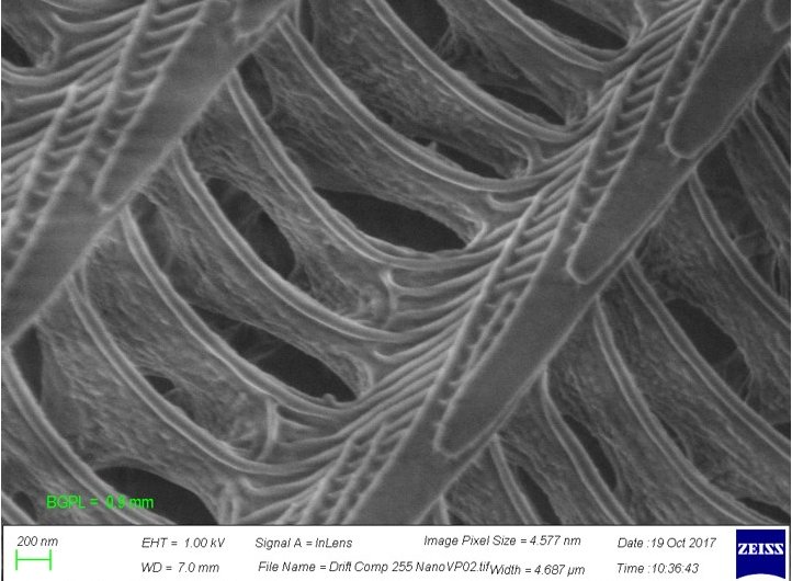
Above is an un-coated wing of a butterfly taken using the variable pressure mode of the SEM. This mode allows some samples to be viewed without coating.
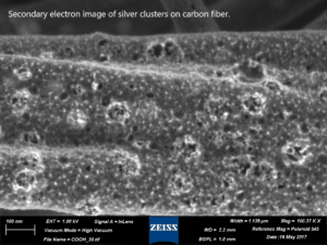
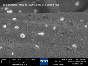
Above is a low voltage secondary electron image of clusters of silver particles on a carbon fiber. It is not clear where the silver particles are. However below is a low-voltage backscattered image of the same sample. The location of the silver clusters is very clear.

Malcolm (Mick) Thomas
607/255-0650
mt57@cornell.edu
Duffield Hall, Room 150
Secondary Contact

Philip Carubia
607/255-6757
pmc228@cornell.edu
Bard Hall, Room SB-56